Datasheet 搜索 > 时钟发生器 > TI(德州仪器) > CDCE72010RGCR 数据手册 > CDCE72010RGCR 数据手册 2/77 页
 器件3D模型
¥ 134.673
CDCE72010RGCR 数据手册 - TI(德州仪器)
制造商:
TI(德州仪器)
分类:
时钟发生器
封装:
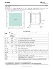
VQFN-64
描述:
十大输出高性能时钟同步器,抖动消除器和时钟经销商 Ten Output High Performance Clock Synchronizer, Jitter Cleaner, and Clock Distributor
Pictures:
3D模型
符号图
焊盘图
引脚图
产品图
页面导航:
导航目录
CDCE72010RGCR数据手册
Page:
of 77 Go
若手册格式错乱,请下载阅览PDF原文件
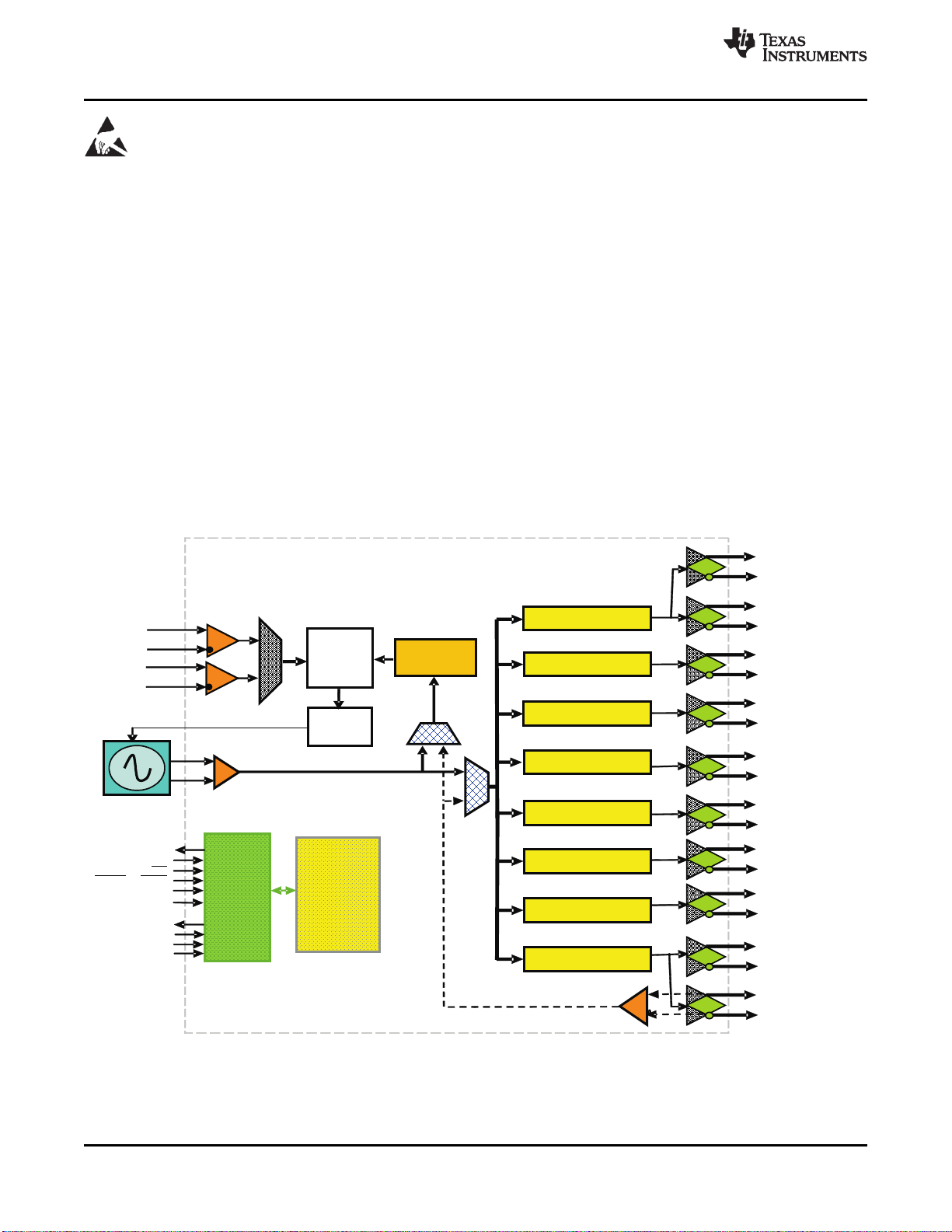
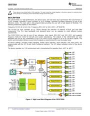
PFD
Charge
Pump
PRI_REF
N
SEC_REF
A
A
u
u
x
x
i
i
l
l
i
i
a
a
r
r
y
y
I
I
n
n
p
p
u
u
t
t
VCXO/ VCO IN
EEPROM
Output Divider 1
U0N
U0P
U1N
U1P
U2N
U2P
U3N
U3P
U4N
U4P
U5N
U5P
U6N
U6P
U7N
U7P
U8N
U8P
U9N or AUXINN
U9P or AUX INP
Output Divider 2
Output Divider 3
Output Divider 4
Output Divider 5
Output Divider 6
Output Divider 7
Output Divider 8
PLL_LOCK
REF_SEL
PD
RESET HOLDor
MODE_SEL
AUX_SEL
SPI_MISO
SPI_LE (CD1)
SPI_CLK (CD2)
SPI_MOSI (CD3)
Interface
& Control
Feedback
Divider
CDCE72010
SCAS858C –JUNE 2008– REVISED JANUARY 2012
www.ti.com
These devices have limited built-in ESD protection. The leads should be shorted together or the device placed in conductive foam
during storage or handling to prevent electrostatic damage to the MOS gates.
DESCRIPTION
The CDCE72010 is a high-performance, low phase noise, and low skew clock synchronizer that synchronizes a
VCXO (Voltage Controlled Crystal Oscillator) or VCO (Voltage Controlled Oscillator) frequency to one of two
reference clocks. The clock path is fully programmable providing the user with a high degree of flexibility. The
following relationship applies to the dividers:
Frequency (VCXO_IN or AUX_IN) / Frequency (PRI_REF or SEC_REF) = (P*N)/(R*M)
The VC(X)O_IN clock operates up to 1.5GHz through the selection of external VC(X)O and loop filter
components. The PLL loop bandwidth and damping factor can be adjusted to meet different system
requirements.
The CDCE72010 can lock to one of two reference clock inputs (PRI_REF and SEC_REF) and supports
frequency hold-over mode for fail-safe and system redundancy. The outputs of the CDCE72010 are user
definable and can be any combination of up to 10 LVPECL/LVDS outputs or up to 20 LVCMOS outputs. The
built-in synchronization latches ensure that all outputs are synchronized for very low output skew.
All device settings, including output signaling, divider value selection, input selection, and many more, are
programmable with the SPI (4-wire Serial Peripheral Interface). The SPI allows individual control of the device
settings.
The device operates in a 3.3V environment and is characterized for operation from –40°C to +85°C.
Figure 1. High Level Block Diagram of the CDCE72010
2 Submit Documentation Feedback Copyright © 2008–2012, Texas Instruments Incorporated
Product Folder Link(s): CDCE72010
器件 Datasheet 文档搜索
AiEMA 数据库涵盖高达 72,405,303 个元件的数据手册,每天更新 5,000 多个 PDF 文件
