Datasheet 搜索 > 时钟发生器 > TI(德州仪器) > CDCE72010RGCR 数据手册 > CDCE72010RGCR 数据手册 6/77 页
 器件3D模型
¥ 134.673
CDCE72010RGCR 数据手册 - TI(德州仪器)
制造商:
TI(德州仪器)
分类:
时钟发生器
封装:
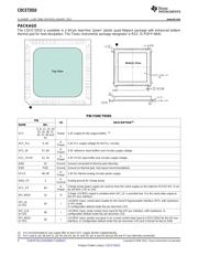
VQFN-64
描述:
十大输出高性能时钟同步器,抖动消除器和时钟经销商 Ten Output High Performance Clock Synchronizer, Jitter Cleaner, and Clock Distributor
Pictures:
3D模型
符号图
焊盘图
引脚图
产品图
页面导航:
导航目录
CDCE72010RGCR数据手册
Page:
of 77 Go
若手册格式错乱,请下载阅览PDF原文件
CDCE72010
SCAS858C –JUNE 2008– REVISED JANUARY 2012
www.ti.com
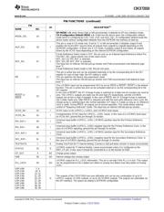
PIN FUNCTIONS (continued)
PIN
I/O DESCRIPTION
(1)
NAME NO.
Positive universal output buffer 9 can be 3-stated and used as a positive universal auxiliary input
U9P or
42 I/O buffer (It requires external termination). The auxiliary input signal can be routed to drive the
AUXINP
outputs or the feedback loop to the PLL.
Negative universal output buffer 9 can be 3-stated and used as a negative universal auxiliary
U9N or
41 I/O input buffer (It requires external termination). The auxiliary input signal can be routed to drive the
AUXINN
outputs or the feedback loop to the PLL.
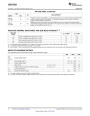
PACKAGE THERMAL RESISTANCE FOR QFN (RGZ) PACKAGE
(1) (2)
AIRFLOW
θ
JP
(°C/W)
(3)
θ
JA
(°C/W)
(LFM)
0 JEDEC compliant board (6×6 VIAs on PAD) 1.5 28
100 JEDEC compliant board (6×6 VIAs on PAD) 1.5 17.6
0 Recommended layout (10×10 VIAs on PAD) 1.5 22.8
100 Recommended layout (10×10 VIAs on PAD) 1.5 13.8
(1) The package thermal impedance is calculated in accordance with JESD 51 and JEDEC2S2P (high-k board).
(2) Connected to GND with 9 thermal vias (0.3 mm diameter).
(3) θ
JP
(Junction – Pad) is used for the QFN package, because the main heat flow is from the junction to the GND-pad of the QFN.
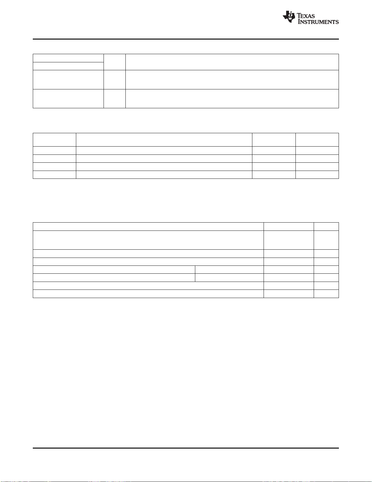
ABSOLUTE MAXIMUM RATINGS
over operating free-air temperature range (unless otherwise noted)
MIN MAX UNIT
V
CC
,
AV
CC
, Supply voltage range
(1)
–0.5 4.6 V
V
CC_CP
V
I
Input voltage range
(2)
–0.5 V
CC
+ 0.5 V
V
O
Output voltage range
(2)
–0.5 V
CC
+ 0.5 V
Input current V
I
< 0, V
I
> V
CC
±20 mA
Output current for LVPECL/LVCMOS Outputs 0 < V
O
< V
CC
±50 mA
T
J
Junction temperature 125 °C
T
stg
Storage temperature range –65 150 °C
(1) All supply voltages have to be supplied simultaneously.
(2) The input and output negative voltage ratings may be exceeded if the input and output clamp-current ratings are observed.
6 Submit Documentation Feedback Copyright © 2008–2012, Texas Instruments Incorporated
Product Folder Link(s): CDCE72010
器件 Datasheet 文档搜索
AiEMA 数据库涵盖高达 72,405,303 个元件的数据手册,每天更新 5,000 多个 PDF 文件
