Datasheet 搜索 > 存储芯片 > Micron(镁光) > MT41J128M16JT-093G:K 数据手册 > MT41J128M16JT-093G:K 数据手册 149/215 页


¥ 13.334
MT41J128M16JT-093G:K 数据手册 - Micron(镁光)
制造商:
Micron(镁光)
分类:
存储芯片
封装:
FBGA-96
描述:
同步动态随机存取内存(SDRAM) MT41J128M16JT-093G:K FBGA-96
Pictures:
3D模型
符号图
焊盘图
引脚图
产品图
页面导航:
原理图在P14P15P150
封装尺寸在P22P23P24P25
标记信息在P1P2
功能描述在P12P13P150P196
技术参数、封装参数在P26P27P31P32P33P34P35P36P37P38P39P40
电气规格在P26P27P31P32P33P34P35P36P37P38P39P40
型号编号列表在P2
导航目录
MT41J128M16JT-093G:K数据手册
Page:
of 215 Go
若手册格式错乱,请下载阅览PDF原文件
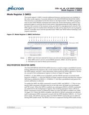
Mode Register 3 (MR3)
The mode register 3 (MR3) controls additional features and functions not available in
the other mode registers. Currently defined is the MULTIPURPOSE REGISTER (MPR).
This function is controlled via the bits shown in the figure below. The MR3 is program-
med via the LOAD MODE command and retains the stored information until it is pro-
grammed again or until the device loses power. Reprogramming the MR3 register will
not alter the contents of the memory array, provided it is reprogrammed correctly. The
MR3 register must be loaded when all banks are idle and no data bursts are in progress,
and the controller must wait the specified time
t
MRD and
t
MOD before initiating a sub-
sequent operation.
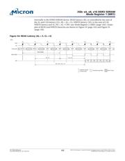
Figure 57: Mode Register 3 (MR3) Definition
A9 A7 A6 A5 A4 A3A8 A2 A1 A0
Mode register 3 (MR3)
Address bus
9765438210
A10A12 A11BA0BA1
101112131415
A13A14
0
1
0
1
0
1
0
1
0
1
0
1
0
1
0
1
MPR
11
BA2
1617
0
1
0
1
0
1
0
1
0
1
M2
0
1
MPR Enable
Normal DRAM operations
2
Dataflow from MPR
MPR_RF
M15
0
1
0
1
M16
0
0
1
1
Mode Register
Mode register set (MR0)
Mode register set 1 (MR1)
Mode register set 2 (MR2)
Mode register set 3 (MR3)
MPR READ Function
Predefined pattern
3
Reserved
Reserved
Reserved
M0
0
1
0
1
M1
0
0
1
1
Notes:
1. MR3[17 and 14:3] are reserved for future use and must all be programmed to 0.
2. When MPR control is set for normal DRAM operation, MR3[1, 0] will be ignored.
3. Intended to be used for READ synchronization.
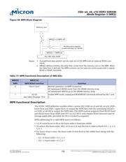
MULTIPURPOSE REGISTER (MPR)
The MULTIPURPOSE REGISTER (MPR) function is used to output a predefined system
timing calibration bit sequence. Bit 2 is the master bit that enables or disables access to
the MPR register, and bits 1 and 0 determine which mode the MPR is placed in. The ba-
sic concept of the multipurpose register is shown in Figure 58 (page 150).
If MR3[2] = 0, then MPR access is disabled, and the DRAM operates in normal mode.
However, if MR3[2] = 1, then the DRAM no longer outputs normal read data but outputs
MPR data as defined by MR3[0, 1]. If MR3[0, 1] = 00, then a predefined read pattern for
system calibration is selected.
To enable the MPR, the MRS command is issued to MR3, and MR3[2] = 1. Prior to issu-
ing the MRS command, all banks must be in the idle state (all banks are precharged,
and
t
RP is met). When the MPR is enabled, any subsequent READ or RDAP commands
are redirected to the multipurpose register. The resulting operation when a READ or
RDAP command is issued, is defined by MR3[1:0] when the MPR is enabled (see Table
78 (page 151)). When the MPR is enabled, only READ or RDAP commands are allowed
until a subsequent MRS command is issued with the MPR disabled (MR3[2] = 0). Power-
down mode, self refresh, and any other non-READ/RDAP commands are not allowed
during MPR enable mode. The RESET function is supported during MPR enable mode.
2Gb: x4, x8, x16 DDR3 SDRAM
Mode Register 3 (MR3)
PDF: 09005aef826aaadc
2Gb_DDR3_SDRAM.pdf - Rev. S 02/16 EN
149
Micron Technology, Inc. reserves the right to change products or specifications without notice.
© 2006 Micron Technology, Inc. All rights reserved.
器件 Datasheet 文档搜索
AiEMA 数据库涵盖高达 72,405,303 个元件的数据手册,每天更新 5,000 多个 PDF 文件
