Datasheet 搜索 > EEPROM芯片 > Xilinx(赛灵思) > XCF01SVOG20C 数据手册 > XCF01SVOG20C 数据手册 2/35 页
 器件3D模型
¥ 103.115
XCF01SVOG20C 数据手册 - Xilinx(赛灵思)
制造商:
Xilinx(赛灵思)
分类:
EEPROM芯片
封装:
TSSOP-20
描述:
XILINX XCF01SVOG20C 芯片, 存储器, PROM, 闪存平台, 1Mb, 20TSSOP
Pictures:
3D模型
符号图
焊盘图
引脚图
产品图
页面导航:
引脚图在P24P25P26P27P28Hot
原理图在P2P34
型号编码规则在P30
标记信息在P30P31P34
封装信息在P13
技术参数、封装参数在P13P24P33P35
应用领域在P35
电气规格在P1P13P16P33


导航目录
XCF01SVOG20C数据手册
Page:
of 35 Go
若手册格式错乱,请下载阅览PDF原文件
Platform Flash In-System Programmable Configuration PROMs
DS123 (v2.18) May 19, 2010 www.xilinx.com
Product Specification 2
R
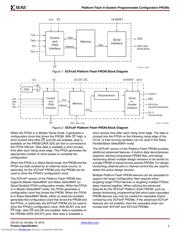
When the FPGA is in Master Serial mode, it generates a
configuration clock that drives the PROM. With CF
High, a
short access time after CE
and OE are enabled, data is
available on the PROM DATA (D0) pin that is connected to
the FPGA DIN pin. New data is available a short access
time after each rising clock edge. The FPGA generates the
appropriate number of clock pulses to complete the
configuration.
When the FPGA is in Slave Serial mode, the PROM and the
FPGA are both clocked by an external clock source, or
optionally, for the XCFxxP PROM only, the PROM can be
used to drive the FPGA’s configuration clock.
The XCFxxP version of the Platform Flash PROM also
supports Master SelectMAP and Slave SelectMAP (or
Slave Parallel) FPGA configuration modes. When the FPGA
is in Master SelectMAP mode, the FPGA generates a
configuration clock that drives the PROM. When the FPGA
is in Slave SelectMAP Mode, either an external oscillator
generates the configuration clock that drives the PROM and
the FPGA, or optionally, the XCFxxP PROM can be used to
drive the FPGA’s configuration clock. With BUSY Low and
CF
High, after CE and OE are enabled, data is available on
the PROMs DATA (D0-D7) pins. New data is available a
short access time after each rising clock edge. The data is
clocked into the FPGA on the following rising edge of the
CCLK. A free-running oscillator can be used in the Slave
Parallel/Slave SelectMAP mode.
The XCFxxP version of the Platform Flash PROM provides
additional advanced features. A built-in data decompressor
supports utilizing compressed PROM files, and design
revisioning allows multiple design revisions to be stored on
a single PROM or stored across several PROMs. For design
revisioning, external pins or internal control bits are used to
select the active design revision.
Multiple Platform Flash PROM devices can be cascaded to
support the larger configuration files required when
targeting larger FPGA devices or targeting multiple FPGAs
daisy chained together. When utilizing the advanced
features for the XCFxxP Platform Flash PROM, such as
design revisioning, programming files which span cascaded
PROM devices can only be created for cascaded chains
containing only XCFxxP PROMs. If the advanced XCFxxP
features are not enabled, then the cascaded chain can
include both XCFxxP and XCFxxS PROMs.
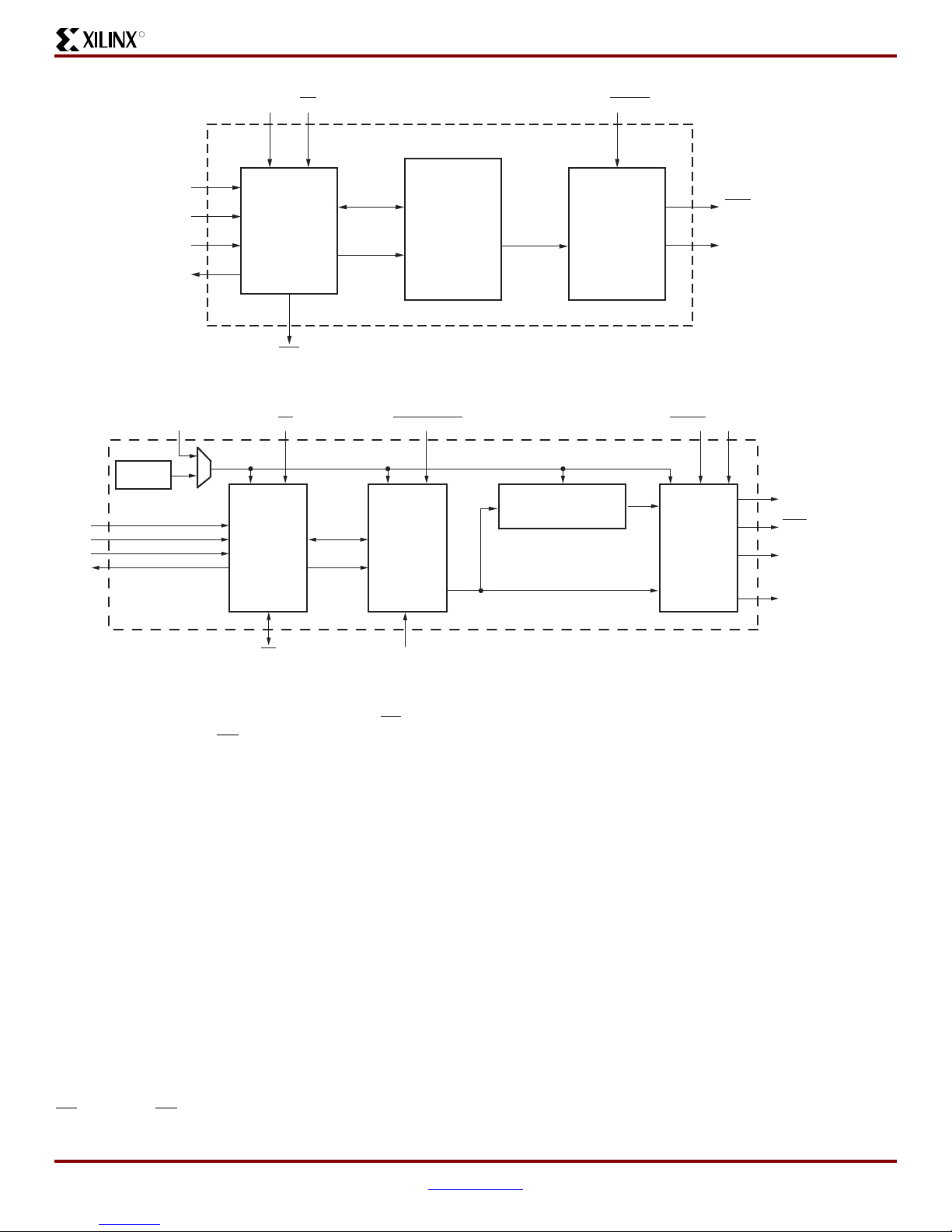
X-Ref Target - Figure 1
Figure 1: XCFxxS Platform Flash PROM Block Diagram
X-Ref Target - Figure 2FI
Figure 2: XCFxxP Platform Flash PROM Block Diagram
Control
and
JTAG
Interface
Memory
Serial
Interface
DATA (D0)
Serial Mode
Data
Address
CLK CE
TCK
TMS
TDI
TDO
OE/RESET
CEO
Data
ds123_01_30603
CF
CLKOUT
CEO
DATA (D0)
(Serial/Parallel Mode)
D[1:7]
(Parallel Mode)
TCK
TMS
TDI
TDO
CLK CE EN_EXT_SEL OE/RESET BUSY
Data
Data
Address
REV_SEL [1:0]
CF
Control
and
JTAG
Interface
Memory
OSC
Serial
or
Parallel
Interface
Decompressor
DS123_19_031908
Downloaded from Elcodis.com electronic components distributor
器件 Datasheet 文档搜索
AiEMA 数据库涵盖高达 72,405,303 个元件的数据手册,每天更新 5,000 多个 PDF 文件
