Datasheet 搜索 > EEPROM芯片 > Xilinx(赛灵思) > XCF01SVOG20C 数据手册 > XCF01SVOG20C 数据手册 3/35 页
 器件3D模型
¥ 103.115
XCF01SVOG20C 数据手册 - Xilinx(赛灵思)
制造商:
Xilinx(赛灵思)
分类:
EEPROM芯片
封装:
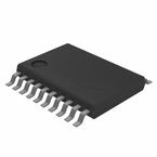
TSSOP-20
描述:
XILINX XCF01SVOG20C 芯片, 存储器, PROM, 闪存平台, 1Mb, 20TSSOP
Pictures:
3D模型
符号图
焊盘图
引脚图
产品图
页面导航:
引脚图在P24P25P26P27P28Hot
原理图在P2P34
型号编码规则在P30
标记信息在P30P31P34
封装信息在P13
技术参数、封装参数在P13P24P33P35
应用领域在P35
电气规格在P1P13P16P33


导航目录
XCF01SVOG20C数据手册
Page:
of 35 Go
若手册格式错乱,请下载阅览PDF原文件
Platform Flash In-System Programmable Configuration PROMs
DS123 (v2.18) May 19, 2010 www.xilinx.com
Product Specification 3
R
See UG161, Platform Flash PROM User Guide, for detailed
guidelines on PROM-to-FPGA configuration hardware
connections, for software usage, for a reference list of Xilinx
FPGAs, and for the respective compatible Platform Flash
PROMs. Ta bl e 2 lists the Platform Flash PROMs and their
capacities.
Programming
The Platform Flash PROM is a reprogrammable NOR flash
device (refer "Quality and Reliability Characteristics,"
page 14 for the program/erase specifications).
Reprogramming requires an erase followed by a program
operation. A verify operation is recommended after the
program operation to validate the correct transfer of data
from the programmer source to the Platform Flash PROM.
Several programming solutions are available.
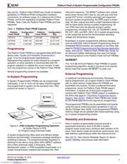
In-System Programming
In-System Programmable PROMs can be programmed
individually, or two or more can be daisy-chained together
and programmed in-system via the standard 4-pin JTAG
protocol as shown in Figure 3.
In-system programming offers quick and efficient design
iterations and eliminates unnecessary package handling or
socketing of devices. The programming data sequence is
delivered to the device using either Xilinx iMPACT software
and a Xilinx download cable, a third-party JTAG
development system, a JTAG-compatible board tester, or a
simple microprocessor interface that emulates the JTAG
instruction sequence. The iMPACT software also outputs
serial vector format (SVF) files for use with any tools that
accept SVF format, including automatic test equipment.
During in-system programming, the CEO
output is driven
High. All other outputs are held in a high-impedance state or
held at clamp levels during in-system programming. All
non-JTAG input pins are ignored during in-system
programming, including CLK, CE, CF, OE/RESET, BUSY,
EN_EXT_SEL, and REV_SEL[1:0]. In-system programming
is fully supported across the recommended operating
voltage and temperature ranges.
Embedded, in-system programming reference designs,
such as X
APP058, Xilinx In-System Programming Using an
Embedded Microcontroller, are available on the Xilinx web
page for P
ROM Programming and Data Storage Application
Notes. See UG161, Platform Flash PROM User Guide, for
an advanced update methodology that uses the Design
Revisioning feature in the Platform Flash XCFxxP PROMs.
OE/RESET
The 1/2/4 Mb XCFxxS Platform Flash PROMs in-system
programming algorithm results in issuance of an internal
device reset that causes OE/RESET
to pulse Low.
External Programming
In traditional manufacturing environments, third-party
device programmers can program Platform Flash PROMs
with an initial memory image before the PROMs are
assembled onto boards. Contact a preferred third-party
programmer vendor for Platform Flash PROM support
information. A sample list of third-party programmer
vendors with Platform Flash PROM support is available on
the Xilinx web page for T
hird-Party Programmer Device
Support. See UG161, Platform Flash PROM User Guide,
for the PROM data file format required for programmers.
Pre-programmed PROMs can be assembled onto boards
using the typical soldering process guidelines in UG112
,
Device Package User Guide. A pre-programmed PROM’s
memory image can be updated after board assembly using
an in-system programming solution.
Reliability and Endurance
Xilinx in-system programmable products provide a
guaranteed endurance level of 20,000 in-system
program-erase cycles and a minimum data retention of 20
years. Each device meets all functional, performance, and
data retention specifications within this endurance limit.
See UG116
, Xilinx Device Reliability Report, for device
quality, reliability, and process node information.
Tabl e 2: Platform Flash PROM Capacity
Platform
Flash PROM
Configuration
Bits
Platform
Flash PROM
Configuration
Bits
XCF01S 1,048,576 XCF08P 8,388,608
XCF02S 2,097,152 XCF16P 16,777,216
XCF04S 4,194,304 XCF32P 33,554,432
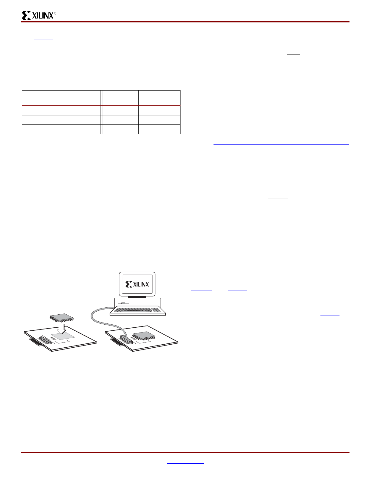
X-Ref Target - Figure 3
Figure 3: JTAG In-System Programming Operation
(a)SolderDevicetoPCB
(b) Program Using Download Cable
DS123_33_031908
GND
V
CC
(a) (b)
Downloaded from Elcodis.com electronic components distributor
器件 Datasheet 文档搜索
AiEMA 数据库涵盖高达 72,405,303 个元件的数据手册,每天更新 5,000 多个 PDF 文件
