Datasheet 搜索 > EEPROM芯片 > Xilinx(赛灵思) > XCF01SVOG20C 数据手册 > XCF01SVOG20C 数据手册 5/35 页
 器件3D模型
¥ 103.115
XCF01SVOG20C 数据手册 - Xilinx(赛灵思)
制造商:
Xilinx(赛灵思)
分类:
EEPROM芯片
封装:
TSSOP-20
描述:
XILINX XCF01SVOG20C 芯片, 存储器, PROM, 闪存平台, 1Mb, 20TSSOP
Pictures:
3D模型
符号图
焊盘图
引脚图
产品图
页面导航:
引脚图在P24P25P26P27P28Hot
原理图在P2P34
型号编码规则在P30
标记信息在P30P31P34
封装信息在P13
技术参数、封装参数在P13P24P33P35
应用领域在P35
电气规格在P1P13P16P33


导航目录
XCF01SVOG20C数据手册
Page:
of 35 Go
若手册格式错乱,请下载阅览PDF原文件
Platform Flash In-System Programmable Configuration PROMs
DS123 (v2.18) May 19, 2010 www.xilinx.com
Product Specification 5
R
IEEE 1149.1 Boundary-Scan (JTAG)
The Platform Flash PROM family is compatible with the IEEE
1149.1 Boundary-Scan standard and the IEEE 1532 in-
system configuration standard. A Test Access Port (TAP) and
registers are provided to support all required Boundary-Scan
instructions, as well as many of the optional instructions
specified by IEEE Std. 1149.1. In addition, the JTAG interface
is used to implement in-system programming (ISP) to facilitate
configuration, erasure, and verification operations on the
Platform Flash PROM device. Table 5 lists the required and
optional Boundary-Scan instructions supported in the
Platform Flash PROMs. Refer to the IEEE Std. 1149.1
specification for a complete description of Boundary-Scan
architecture and the required and optional instructions.
Caution!
The XCFxxP JTAG TAP pause states are not fully
compliant with the JTAG 1149.1 specification. If a temporary
pause of a JTAG shift operation is required, then stop the
JTAG TCK clock and maintain the JTAG TAP within the JTAG
Shift-IR or Shift-DR TAP state. Do not transition the XCFxxP
JTAG TAP through the JTAG Pause-IR or Pause-DR TAP state
to temporarily pause a JTAG shift operation.
Instruction Register
The Instruction Register (IR) for the Platform Flash PROM
is connected between TDI and TDO during an instruction
scan sequence. In preparation for an instruction scan
sequence, the instruction register is parallel loaded with a
fixed instruction capture pattern. This pattern is shifted out
onto TDO (LSB first), while an instruction is shifted into the
instruction register from TDI.
XCFxxS Instruction Register (8 bits wide)
The Instruction Register (IR) for the XCFxxS PROM is eight
bits wide and is connected between TDI and TDO during an
instruction scan sequence. The detailed composition of the
instruction capture pattern is illustrated in Table6, page6.
The instruction capture pattern shifted out of the XCFxxS
device includes IR[7:0]. IR[7:5] are reserved bits and are set
to a logic 0. The ISC Status field, IR[4], contains logic 1 if
the device is currently in In-System Configuration (ISC)
mode; otherwise, it contains logic 0. The Security field,
IR[3], contains logic 1 if the device has been programmed
with the security option turned on; otherwise, it contains
logic 0. IR[2] is unused, and is set to '0'. The remaining bits
IR[1:0] are set to '01' as defined by IEEE Std. 1149.1.
XCFxxP Instruction Register (16 bits wide)
The Instruction Register (IR) for the XCFxxP PROM is sixteen
bits wide and is connected between TDI and TDO during an
instruction scan sequence. The detailed composition of the
instruction capture pattern is illustrated in Table 7, page 6.
The instruction capture pattern shifted out of the XCFxxP
device includes IR[15:0]. IR[15:9] are reserved bits and are set
to a logic 0. The ISC Error field, IR[8:7], contains a 10 when an
ISC operation is a success; otherwise a 01 when an In-System
Configuration (ISC) operation fails. The Erase/Program
(ER/PROG) Error field, IR[6:5], contains a 10 when an erase
or program operation is a success; otherwise a 01 when an
erase or program operation fails. The Erase/Program
(ER/PROG) Status field, IR[4], contains a logic 0 when the
device is busy performing an erase or programming operation;
otherwise, it contains a logic 1. The ISC Status field, IR[3],
contains logic 1 if the device is currently in In-System
Configuration (ISC) mode; otherwise, it contains logic 0. The
DONE field, IR[2], contains logic 1 if the sampled design
revision has been successfully programmed; otherwise, a logic
0 indicates incomplete programming. The remaining bits
IR[1:0] are set to 01 as defined by IEEE Std. 1149.1.
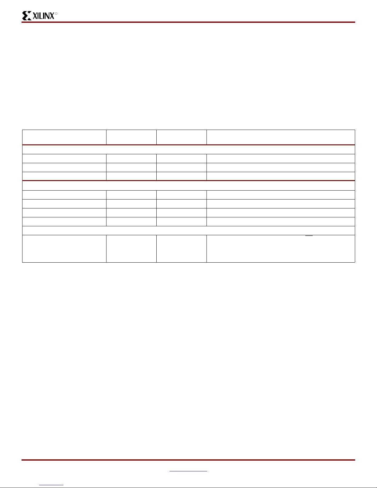
Tabl e 5: Platform Flash PROM Boundary-Scan Instructions
Boundary-Scan Command
XCFxxS IR[7:0]
(hex)
XCFxxP IR[15:0]
(hex)
Instruction Description
Required Instructions
BYPASS FF FFFF Enables BYPASS
SAMPLE/PRELOAD 01 0001 Enables Boundary-Scan SAMPLE/PRELOAD operation
EXTEST 00 0000 Enables Boundary-Scan EXTEST operation
Optional Instructions
CLAMP FA 00FA Enables Boundary-Scan CLAMP operation
HIGHZ FC 00FC Places all outputs in high-impedance state simultaneously
IDCODE FE 00FE Enables shifting out 32-bit IDCODE
USERCODE FD 00FD Enables shifting out 32-bit USERCODE
Platform Flash PROM Specific Instructions
CONFIG EE 00EE
Initiates FPGA configuration by pulsing CF
pin Low once.
(For the XCFxxP this command also resets the selected
design revision based on either the external REV_SEL[1:0]
pins or on the internal design revision selection bits.)
(1)
Notes:
1. For more information see "Initiating FPGA Configuration," page 10.
Downloaded from Elcodis.com electronic components distributor
器件 Datasheet 文档搜索
AiEMA 数据库涵盖高达 72,405,303 个元件的数据手册,每天更新 5,000 多个 PDF 文件
