Datasheet 搜索 > CPLD芯片 > Altera(阿尔特拉) > EPM240T100I5N 数据手册 > EPM240T100I5N 数据手册 3/10 页
 器件3D模型
¥ 24.435
EPM240T100I5N 数据手册 - Altera(阿尔特拉)
制造商:
Altera(阿尔特拉)
分类:
CPLD芯片
封装:
TQFP-100
描述:
ALTERA EPM240T100I5N 芯片, CPLD, MAX II, 240单元, TQFP100
Pictures:
3D模型
符号图
焊盘图
引脚图
产品图
页面导航:
应用领域在P10

导航目录
EPM240T100I5N数据手册
Page:
of 10 Go
若手册格式错乱,请下载阅览PDF原文件
Altera Corporation 3
Preliminary
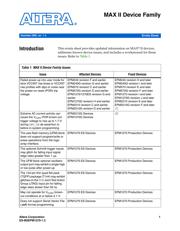
EPM2210G & EPM1270G Brown-out Voltage Issue
The MAX II POR circuitry is enhanced in later revisions to withstand
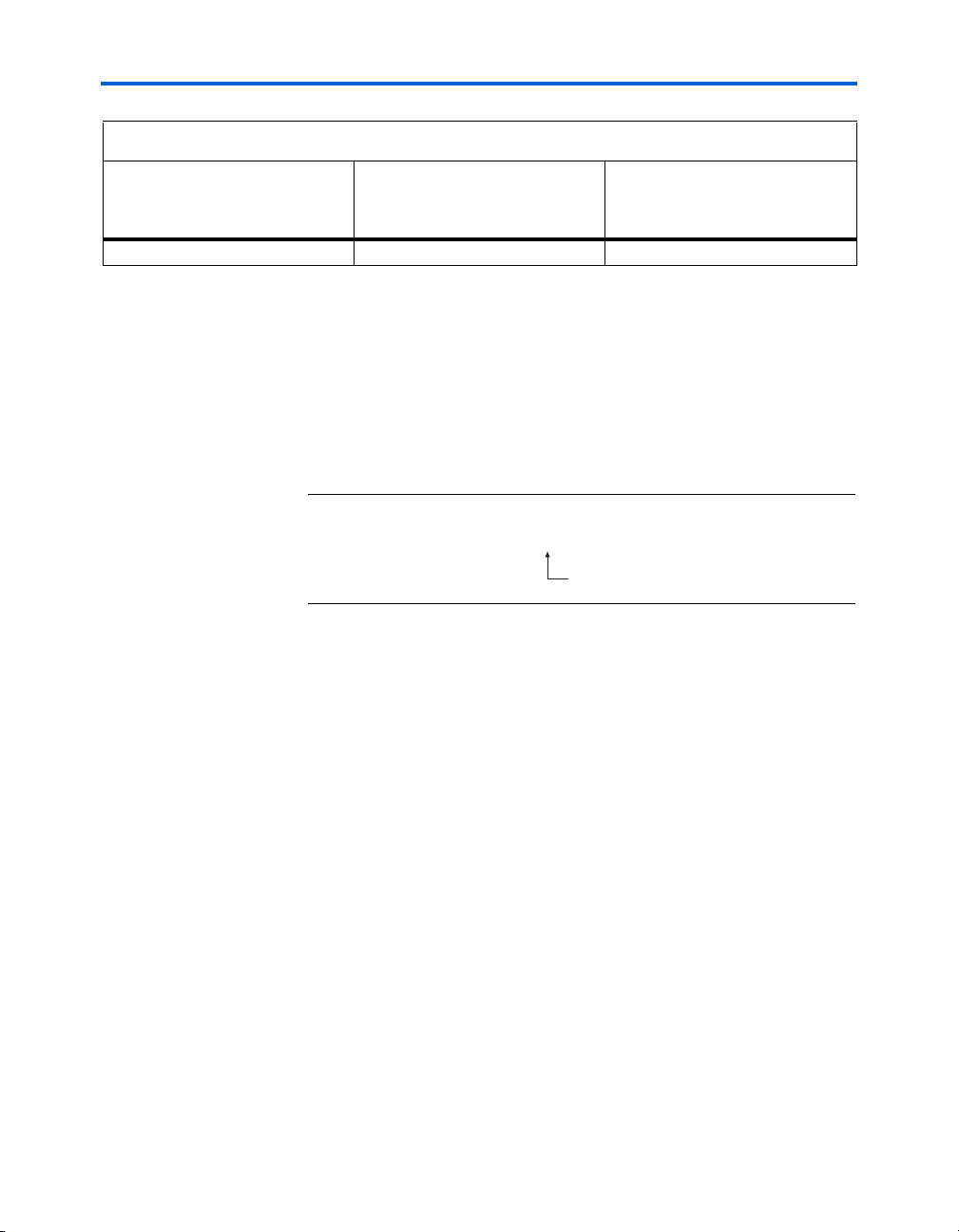
non-monotonic, slow rise times in the revision codes that are shown in
Table 1. The die revision is identified by the alphanumeric character (Z)
before the fab code (first two alphanumeric characters) in the data code
printed on the top side of the device. Figure 1 shows a MAX II device's
top side date code.
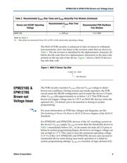
Figure 1. MAX II Device Top Side
EPM2210G &
EPM1270G
Brown-out
Voltage Issue
The POR circuitry monitors V
CCINT
(but not V
CCIO
) voltage to detect
brown-out conditions. During normal user-mode operation, the POR
circuit resets the SRAM configuration and tri-states the device I/O pins
when V
CCINT
falls approximately to or below 1.4 V. This POR circuit
brown-out trigger voltage rises to 1.55 V on MAX IIG devices when the
optional DEV_OE feature/pin is de-asserted or during in-system
programming.
f For more information on POR trip voltages and diagrams, see the
Hot-Socketing & Power-On Reset in MAX II Devices chapter of the MAX II
Handbook.
For EPM2210G and EPM1270G devices, if the AC switching current on
the device’s V
CCINT
supply (I
CCINT
) is more than the thresholds shown in
Table 3 immediately before DEV_OE de-asserts (tri-state all I/O pins) or
before in-system programming begins, the brown-out trigger voltage can
rise as high as 1.7 V. This value is near the minimum operating voltage
(1.71 V) of the 1.8-V EPM2210G and EPM1270G devices and can lead to
unintended device reset during user-mode operation or a failed in-
system programming attempt. I
CCINT
is a function of logic element (LE)
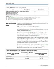
MAX IIG <= 540 µs 1.3-1.65V
Note to Ta ble 2:
(1) Rise times are measured from 10% to 90% of the stead-state operating voltage.
Table 2. Recommended V
CCINT
Rise Times and V
CCINT
Noise/Dip Free Window (Continued)
Device and VCCINT Operating
Voltage
Recommended V
CCINT
Rise Time
(1)
Recommended POR Dip/Noise
Free Window
A Xβ
Z
## ####
Die Revision
器件 Datasheet 文档搜索
AiEMA 数据库涵盖高达 72,405,303 个元件的数据手册,每天更新 5,000 多个 PDF 文件
