Datasheet 搜索 > CPLD芯片 > Altera(阿尔特拉) > EPM240T100I5N 数据手册 > EPM240T100I5N 数据手册 6/10 页
 器件3D模型
¥ 24.435
EPM240T100I5N 数据手册 - Altera(阿尔特拉)
制造商:
Altera(阿尔特拉)
分类:
CPLD芯片
封装:
TQFP-100
描述:
ALTERA EPM240T100I5N 芯片, CPLD, MAX II, 240单元, TQFP100
Pictures:
3D模型
符号图
焊盘图
引脚图
产品图
页面导航:
应用领域在P10

导航目录
EPM240T100I5N数据手册
Page:
of 10 Go
若手册格式错乱,请下载阅览PDF原文件

6 Altera Corporation
Preliminary
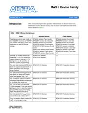
MAX II Device Family
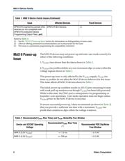
If the OSCENA port is asserted at the power-up condition in the design, the
OSC output port does not exhibit a high or low pulse, but instead
immediately starts clocking upon entry into user mode. For the asserted
or de-asserted OSCENA power-up possibilities, it is undetermined
whether the OSC output starts with a rising or falling edge. You should
assume an unknown “X” on the OSC output port for all power-up
conditions in your design with EPM1270 ES devices.
1 Production devices do not exhibit the high or low pulse after
power-up for the de-asserted OSCENA signal. For these devices,
OSC stays high at power-up and does not clock until enabled
with OSCENA.
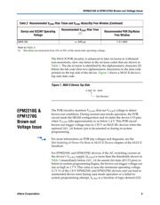
Schmitt Trigger Slow Falling Input Edge Glitch
The Schmitt trigger input buffer is an optional feature on each I/O pin in
MAX II devices to help maximize noise immunity on input pins. For
EPM1270 ES devices, the 3.3-V or 2.5-V Schmitt trigger input option may
glitch when driven by high-to-low signal transitions with fall times
greater than 1 µs. Low-to-high signal transitions are not susceptible to
glitch and reliably accept signals with rise times up to 200 ms.
The workaround to improve the Schmitt trigger falling edge input
performance beyond 1-µs fall times is to enable the programmable input
delay for that particular pin. Enabling the programmable input delay for
the input pin allows the Schmitt trigger to accept fall times up to 200 ms.
The programmable input delay adds a delay to the input delay path of
~2.1 ns for -4 speed grade and ~2.6 ns for -5 speed grade. This option can
be set in the Assignment Editor (Assignments menu) on a pin-by-pin
basis. The procedure to set this in the Quartus II software for a pin is
shown below:
1. Select input pin name in the design file.
2. Right-click and select Locate in Assignment Editor.
3. Double-click the cell under Assignment Name and select Input
Delay from Pin to Internal Cells in the drop-down list.
4. Double-click the Va lu e cell to the right of the assignment name just
made and enter 1.
5. Click Save (File menu).
This procedure turns on the input delay for the selected input pin.
器件 Datasheet 文档搜索
AiEMA 数据库涵盖高达 72,405,303 个元件的数据手册,每天更新 5,000 多个 PDF 文件
